
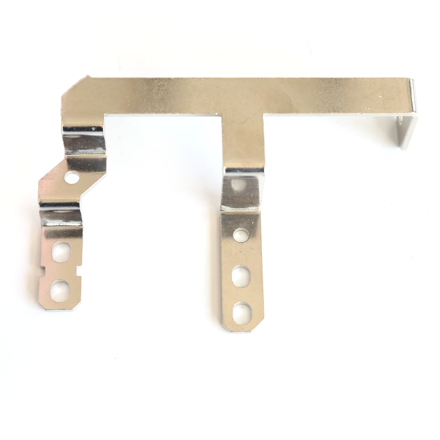
Precision Metal Stamping for Miniaturized Electronic Components
The Role of Micro-Precision Stamping in Compact Devices
The micro precision metal stamping technique makes possible large scale manufacturing of super thin components below 0.2mm thickness. These tiny parts are vital across many industries including smartphones, medical devices, and internet connected sensors. With modern progressive die technology, manufacturers can get tolerances down to around 5 microns or better. This level of accuracy keeps connector pins working properly even when exposed to moisture or constant vibrations. The market research firm Future Market Insights reports that roughly two thirds of consumer electronics companies have started favoring stamped metal components instead of plastic ones for their most important connections. Metal just lasts longer and conducts electricity much better than plastics do, which explains why so many manufacturers are making the switch despite higher initial costs.
Semiconductor Lead Frames and Micron-Level Tolerance Challenges
Semiconductor lead frames require stamping precision within ±2 microns—where even 0.5-micron deviations can cause 15% signal loss in high-frequency chips. Laser-guided presses with real-time adjustment systems reduce dimensional drift by 40% during continuous production, supporting reliable fabrication of 5G modems at 1.5 million units per month.
Innovations Pushing the Limits of Component Miniaturization
Three key advancements are driving miniaturization:
- Hybrid stamping-etching processes producing 0.08mm-thick EMI shields
- Multi-stage dies forming waterproof seals during connector fabrication
- AI-powered vision systems detecting sub-micron defects at 2,000 parts/minute
These innovations allow wearables to shrink by 22% in footprint while doubling battery capacity.
Why Metal Stamping Parts Are Critical in High-Density Electronics
Stamped components deliver 360° EMI shielding for millimeter-wave 5G antennas and offer 50% better heat dissipation than polymers in processors drawing over 30W. Their compatibility with SMT assembly lines eliminates secondary fastening steps, reducing overall device thickness.
Case Example: Stamped Components in Smartphones and Wearables
A flagship 5G smartphone contains 127 stamped parts—from 0.3mm antenna brackets to corrosion-resistant SIM trays. Fitness trackers use titanium-stamped biosensor contacts that endure 12,000 flex cycles while maintaining less than 0.5Ω resistance, enabling continuous health monitoring even in saltwater environments.
Key Metal Stamping Processes Driving Electronics Manufacturing
Progressive Die Stamping for High-Volume Electronic Connectors
Progressive die stamping dominates high-volume connector manufacturing, producing up to 1,500 parts per minute. Multi-stage tooling simultaneously punches, bends, and forms raw metal strips, achieving ±3-micron dimensional consistency (Manufacturing Tech Report 2023). This precision ensures reliable conductivity and mating performance in USB-C ports and memory card slots.
Blanking, Coining, and Their Applications in Metal Stamping Parts
Blanking cuts final shapes from sheet metal with 99.2% material utilization, ideal for SIM trays and shielding plates. Coining achieves sub-0.1µm surface roughness for charging contacts, ensuring optimal electrical performance without secondary polishing. Together, these processes account for 68% of stamped parts in modern PCB assemblies.
Achieving Consistent Precision in High-Speed Stamping Lines
Advanced 400-ton servo presses maintain ±1.5µm tolerances at 1,200 strokes/minute using real-time force monitoring and adaptive toolpath correction. Temperature-controlled dies prevent thermal drift in 5G antenna brackets, while inline laser scanners verify hole alignment within 5µm—essential for millimeter-wave frequency stability.
Integration of Stamping Processes in Automated Electronics Assembly
Robotic handlers feed stamped EMI shields and connector pins directly into SMT machines, cutting assembly cycle times by 34% (Automation Today 2023). This closed-loop integration supports high-precision manufacturing of smartwatch chassis and IoT sensor housings, where tight tolerances prevent moisture ingress and signal interference.
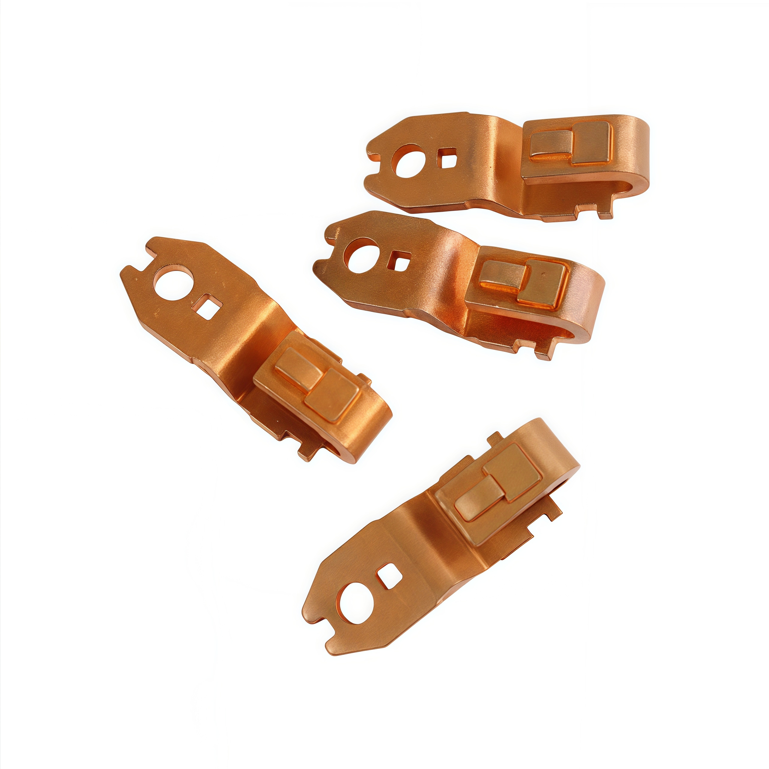
Materials and Design Considerations for Electronic Metal Stamping
Common Materials: Copper, Brass, and Aluminum in Stamped Components
When it comes to metal stamping in electronics, copper, brass, and aluminum are the big three thanks to their special characteristics. Copper stands out because it conducts electricity so well, which makes it great for things like connectors and various circuit parts. Brass has this nice middle ground between being resistant to rust and easy to work with during manufacturing. Aluminum brings something different to the table too its light weight combined with decent strength makes it perfect for heat sinks and other structural bits inside devices. Looking at industry trends, around two thirds of all consumer electronics these days actually incorporate stamped aluminum components somewhere inside them, mainly for managing heat dissipation and keeping overall product weights down.
Material Selection for Conductivity, Thermal Management, and Durability
Engineers evaluate three key factors:
- Conductivity: Copper’s 100% IACS rating ensures efficient signal transfer in high-frequency devices
- Thermal performance: Aluminum dissipates heat 50% faster than steel, crucial for compact 5G infrastructure
- Durability: Brass withstands wear in high-cycle applications like USB port contacts
These criteria support the development of smaller, higher-performance electronics requiring robust thermal and electrical behavior.
Case Study: Aluminum vs. Copper in Heat Sink and Shielding Applications
A 2023 analysis found aluminum’s 30% weight advantage compensates for its 40% lower conductivity in smartphone shielding. However, copper remains the preferred choice for high-power server heat sinks handling over 150W. Hybrid designs combining both materials achieve 22% better thermal efficiency than single-metal solutions.
Advanced Alloys and Future Material Trends in Metal Stamping Parts
Oxygen-free copper alloys and silicon-aluminum composites enable stamped components to handle 15% higher current loads while reducing electromagnetic interference. Industry forecasts predict a 12% annual growth in demand for beryllium-copper alloys, particularly in aerospace-grade RF shielding through 2030. These developments solidify metal stamping’s role in next-generation electronics miniaturization.
EMI/RFI Shielding and Structural Applications of Stamped Metal Parts
Metal stamping parts are essential for mitigating electromagnetic and radio frequency interference in modern electronics. By combining precision manufacturing with conductive materials like aluminum and copper, stamped components achieve shielding effectiveness of 40–60 dB attenuation in critical frequency bands, ensuring compliance with IEC 61000 and FCC standards.
Design and Production of Stamped Metal Enclosures for EMI/RFI Shielding
These enclosures use materials optimized for conductivity and permeability. Aluminum shields ≥85% of high-frequency EMI (20–50 GHz) in 5G infrastructure, while copper excels at low-frequency (30–300 MHz) shielding in IoT sensors. Progressive die stamping produces enclosures with <50 μm dimensional tolerances, preserving Faraday cage integrity in medical monitors and automotive control units.
Stamped Battery Contacts, Connector Pins, and Shielding Cases
Beyond shielding, stamped parts provide structural support in confined spaces. Nickel-coated steel battery contacts resist oxidation and maintain <10 mΩ resistance, while gold-plated connector pins preserve signal integrity in high-speed data transmission. Multistage forming enables complex geometries for snap-fit shielding cases in miniature Bluetooth modules.
Growing Demand for Shielded Components in 5G and IoT Devices
The 2024 Metal Stamping Market Analysis projects a 15% annual growth in EMI/RFI components, driven by 5G mmWave (24–47 GHz) adoption and IoT proliferation. Smart factories now integrate AI-driven toolpath optimization to produce 5G antenna shielding with ±8 μm accuracy at 1,200 parts/minute.
Performance Benefits of Metal Stamping Parts in Sensitive Electronics
Metal stamped shields cut down on EMI leakage around 93% in those millimeter wave radar setups when compared against plastic options. For satellites talking across space, beryllium copper springs keep good grounding connections even after going through extreme temps ranging from minus 40 degrees all the way up to plus 125 Celsius. The dependable nature of these stamped parts means they show up everywhere from aircraft electronics to surgically implanted medical gear, places where things just can't fail no matter what happens.
Automation, Innovation, and Future Trends in Electronic Metal Stamping
Smart Factories: CNC, Automation, and Real-Time Quality Control
Stamping plants today run about 85 percent more efficiently compared to what they were back in 2018, thanks largely to advances in automated systems. These modern facilities use servo driven CNC presses capable of achieving around plus or minus 2 microns precision, allowing them to produce tiny socket connectors and various shielding components non stop throughout the day and night. The latest real time vision inspection systems can spot flaws as small as 0.1 millimeters, cutting down on wasted materials significantly. For instance, manufacturers report seeing roughly a 63% drop in defective parts for battery contacts and RF shielding components, based on findings from industry reports published last year.
AI-Driven Design and Process Optimization in Metal Stamping
Machine learning algorithms predict material springback with 97% accuracy, enabling first-pass success in 82% of lead frame stamping operations. These models analyze over 15 variables—including strip thickness, alloy composition, and press forces—addressing the root cause of 56% of shielding case defects (ThomasNet 2023).
Sustainable Stamping and Cost-Efficiency in High-Precision Lines
Advanced servo presses cut energy use by 40% compared to mechanical systems while sustaining 1,200 strokes/minute. Material utilization exceeds 93% in progressive die lines through AI-optimized nesting, a critical advantage when working with costly alloys like beryllium copper in 5G millimeter-wave antennas.
Future Outlook: Customization and Advanced Applications in 5G Infrastructure
The deployment of 38GHz+ 5G networks demands waveguide components with surface finishes below 0.4Ra—achievable only through hybrid stamping-laser ablation. Industry forecasts anticipate 300% growth in millimeter-wave shielding cases by 2028, with customized metal stamping parts forming the foundation of next-gen base station designs.
FAQ
What is micro precision metal stamping?
Micro precision metal stamping is a technique used to manufacture extremely thin metal components with high accuracy, typically below 0.2mm thickness, which are essential for industries such as electronics and medical devices.
Why are stamped metal components favored over plastic ones in electronics?
Stamped metal components are preferred because they offer better durability and conductivity compared to plastics, leading to longer-lasting connections and superior electrical performance.
What are the common materials used in metal stamping for electronics?
The common materials include copper, brass, and aluminum. Copper is chosen for its excellent conductivity, brass for its corrosion resistance while being easy to work with, and aluminum for its lightweight and strength.
How do innovations in stamping processes support electronics miniaturization?
Innovations such as hybrid stamping-etching processes, multi-stage dies, and AI-powered vision systems enable the production of smaller, more efficient electronic components by enhancing precision and detecting defects.
Table of Contents
-
Precision Metal Stamping for Miniaturized Electronic Components
- The Role of Micro-Precision Stamping in Compact Devices
- Semiconductor Lead Frames and Micron-Level Tolerance Challenges
- Innovations Pushing the Limits of Component Miniaturization
- Why Metal Stamping Parts Are Critical in High-Density Electronics
- Case Example: Stamped Components in Smartphones and Wearables
- Progressive Die Stamping for High-Volume Electronic Connectors
- Blanking, Coining, and Their Applications in Metal Stamping Parts
- Achieving Consistent Precision in High-Speed Stamping Lines
- Integration of Stamping Processes in Automated Electronics Assembly
- Materials and Design Considerations for Electronic Metal Stamping
- EMI/RFI Shielding and Structural Applications of Stamped Metal Parts
- Automation, Innovation, and Future Trends in Electronic Metal Stamping
- FAQ