
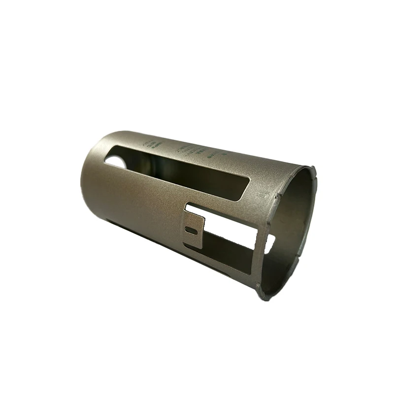
The art of micro precision metal stamping makes it possible to produce all those tiny but vital parts that keep our modern gadgets running smoothly. Recent industry data from last year shows that today's smartphones actually contain more than eighty different stamped metal pieces. Think about those super thin SIM card slots at just 0.8 millimeters thick or those almost invisible antenna brackets that are literally thinner than a strand of human hair. What's really impressive is how accurately these parts get made, often within tolerances below five microns which is plus or minus 0.005 millimeters. That kind of accuracy matters a lot for things like 5G phone connectors where even the slightest misalignment can mess up signal quality. With multi stage progressive dies, manufacturers can shape electrical contacts and design ventilation patterns right into laptop heat sinks all at once, getting both function and form done in one go. And let's not forget the speed factor either these machines can crank out over 1,200 parts every single minute without losing track of quality, even when making runs of ten million units or more. When compared to methods like laser cutting, this stamping approach definitely wins when it comes to scaling up production efficiently.
Progressive die stamping allows multiple operations like cutting, bending, and shaping all at once during one press cycle. That's why manufacturers love using this approach for producing large quantities of electronic connectors. The process can hit speeds over 1,200 strokes each minute while maintaining position accuracy down to about plus or minus 0.05 mm. Pretty impressive stuff considering how small components like USB-C ports and SIM card slots need such tight tolerances. According to recent manufacturing reports, companies adopting progressive stamping cut down on extra processing steps by around 40% compared to older stamping techniques. This makes a big difference particularly when making delicate parts such as contact springs and those metal shields that protect sensitive electronics from interference.
Progressive die systems have this built-in ability to repeat processes consistently, which means manufacturers can crank out over 10 million parts each month. And guess what? The cost per part stays below ten cents for those basic connectors most companies need. When it comes to feeding materials into these systems, modern technology gets really efficient. We're talking about material usage rates that hit around 92% or better for copper alloys and phosphor bronze stuff. That kind of efficiency matters a lot when making components for 5G antennas and battery terminals where every penny counts. Press machines now come packed with IoT sensors too. These smart devices help cut down on cycle times by roughly 15-20% and keep an eye on how tools are wearing down throughout production runs.
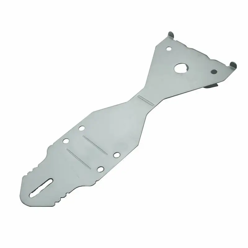
Fine blanking works really well for making EMI shielding cans and those tiny micro-SD card housings. The process creates nice clean edges with surface roughness below around 3.2 microns Ra. When it comes to compound dies, they basically do two things at once - pierce and extrude - which is great for creating those gold plated contact pins that need to fit within tight 0.2mm pitch tolerances. Manufacturers have made some pretty cool progress lately too. Now they can make multi level heat sinks all in one go with built in mounting clips and thermal channels. This cuts down on 3 to 5 separate assembly steps when building server components, saving both time and money in the production process.
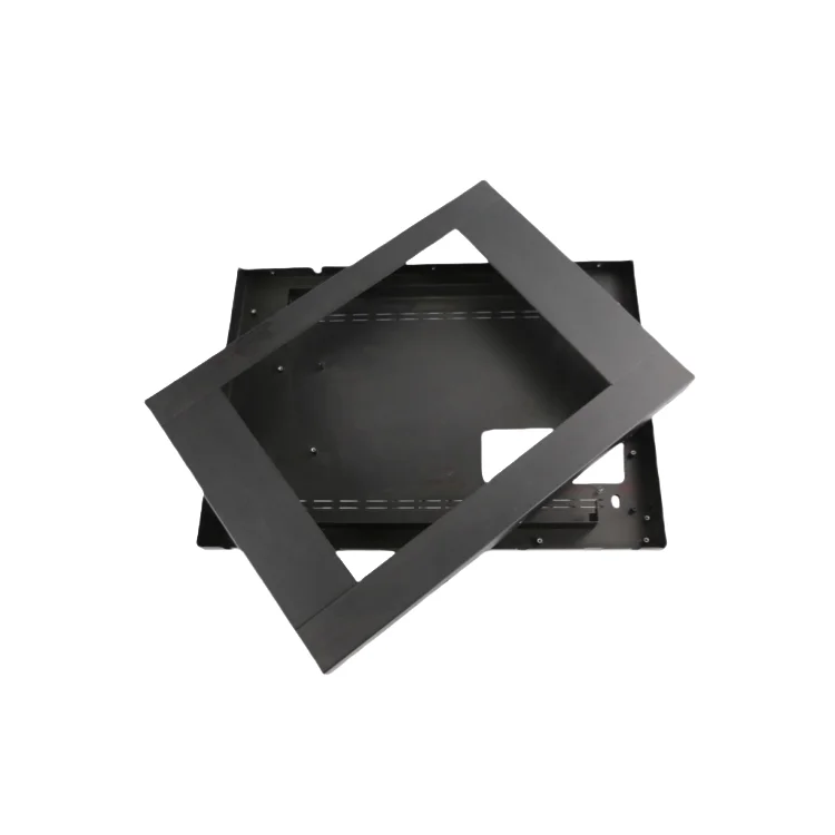
Metal enclosures stamped from conductive materials such as copper or aluminum alloys help fight against electromagnetic interference (EMI) and radio frequency interference (RFI). These materials reflect incoming signals while certain types of ferrous stainless steel absorb leftover energy. Even small gaps matter a lot here though. If there are openings bigger than 0.3 mm, shielding performance drops significantly around 40 dB at 1 GHz frequencies. That's why precision matters so much in stamping processes which now commonly achieve tolerances within plus or minus 0.05 mm. The rise of 5G networks along with all those Internet of Things devices on the market has led to a noticeable uptick in demand for these shielding components. Industry reports show about a 22% increase since 2022 actually. Most manufacturers today focus on creating enclosure designs where grounding features are built right in from the start rather than added later.
Three factors dominate shielding performance:
| Factor | High-Performance Example | Tradeoff Consideration |
|---|---|---|
| Conductivity | Copper (100% IACS*) | Higher cost vs. aluminum |
| Corrosion Resistance | 304 Stainless Steel | 18% lower conductivity |
| Formability | Annealed Aluminum 6061 | Thinner gauges risk denting |
*International Annealed Copper Standard
Designers must optimize enclosure geometry to eliminate sharp corners—responsible for 90% of EM leakage points in consumer electronics—while maintaining spring-loaded contact points for consistent conductivity under vibration. In automotive applications, stamped shielding parts now withstand temperature cycles from -40°C to 125°C without performance degradation.
These days, electronic devices depend heavily on stamped parts that do more than one job at once, combining structural strength with the ability to conduct electricity. Take EMI shielding plates for instance. Many manufacturers are now designing them to also serve as the frame for 5G router housings. This cuts down on how many separate parts need to be made and assembled, which is a big deal when trying to keep production costs under control. According to research published last year across several industries, around two thirds of companies making telecom gear have adopted this approach. The main reason? It makes putting together complex equipment much simpler, especially when dealing with tight spaces inside modern devices.
Smartphones exemplify this trend through:
Engineers optimize multi-functional designs using copper-beryllium alloys, which balance 80,000 PSI tensile strength with 98% IACS conductivity. Laser-etched surface patterns maintain electrical contact integrity after 50,000+ flex cycles in folding-screen devices. Simulation-driven designs now achieve <0.1Ø resistance variance under ±5% mechanical stress—a critical benchmark for automotive sensor applications.
Micro precision metal stamping is a process that produces small and highly accurate metal parts, often used in electronic components like smartphones and laptops. It involves shaping metal with high precision within tight tolerance levels.
Progressive die stamping combines multiple operations like cutting, bending, and shaping into one press cycle, allowing for high-speed production of electronic connectors with consistent accuracy. It reduces extra processing steps and production costs.
Material selection, such as using copper for high conductivity, along with precise stamping that eliminates gaps larger than 0.3 mm, ensures effective EMI/RFI shielding. Designed grounding features enhance performance by maintaining tight tolerances.
Multi-functional integration reduces the number of separate parts needed, thus simplifying assembly processes and reducing production costs while saving space within electronic devices.
Cangzhou Deeplink delivers precision metal stamping, sheet fabrication, and hardware solutions for global high-end manufacturing. Our full-chain services ensure fast delivery, exquisite craftsmanship, and stable quality. Contact us for customized quotes!
The West Area Of The Economic Development Zone of Nanpi County, Cangzhou City, Hebei Province
Copyright © 2025 by Cangzhou Deeplink International Supply Chain Co., Ltd. Privacy Policy
 Hot News